Defect Detection in Manufacturing


AI-supported optical defect detection for semiconductor laser production.

Input

Images of semiconductors

Output

Type and location of defects

Goal

Increase the efficiency of the defect inspection


Introduction


A major challenge of the semiconductor industry is quality control. The visual inspection of components requires trained employees and maximum concentration, but is also monotonous and tiring. We are developing an automated process to detect defects in the production process in real-time.


Starting Point


The three industrial manufacturers of laser diodes that are involved in this project as well as the Ferdinand-Braun-Institut, Leibniz-Institut für Höchstfrequenztechnik (FBH) face the typical challenges of the semiconductor industry in their production processes.

Rigid quality control is mandatory due to the downstream costs of defect components. While defects and defect types can be clearly identified via visual inspection, there is high personnel and financial expenditure for those inspections. In large parts, an inspection is carried out by a trained employee. It is a task that requires the highest concentration and care, but at the same time, it is monotonous and tiring.

The goal of the LaserSKI project is to solve these challenges by applying machine learning to detect and classify the defects in different stages of the production process automatically. This will

  • increase the efficiency and reliability of the defect inspection

  • lower costs

  • relieve employees from monotonous quality control tasks

  • enable companies to detect patterns in defect occurrence in real-time.

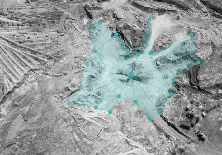
Automatic tagging of the defects on semiconductors: The algorithm detects different kind of defects.


Challenges


The data is divided into two broad categories

  • facet images showing a cross-section of the semiconductor

  • p-side images showing it from above (see image above and below).

Each of these has a different set of challenges. In particular, the p-side data has a complex etched structure that makes conventional computer vision difficult. In the facet data, defects can vary significantly in size and colour.

Automatically classified levels of defect: Example of p-side inspection with different severity of defects (image: FBH).


Solution


We use separate models for each class of data, both of which are based on a convolutional neural network. These models detect and classify the defects.

The output of the models will be passed to a rules-based system that determines the severity of the defects based on their class and location within the image. The final result is returned both as an image with the regions highlighted and a CSV file containing the classes and locations of the defects.

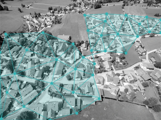
Automatic laser diode inspection using machine learning: Example of laser diode facet inspection with different types of defects.


Technical Background


Challenges

There are a number of difficulties unique to this project compared with other computer vision projects:

  • Bimodal data: We have two disjoint datasets: p-side and facet which share some but not all possible defects.

  • The scale of defects: these can range from a few pixels to significant proportions of the image which can be thousands of pixels across.

  • Background structure: the p-side, in particular, has an elaborate etched structure that makes using classical computer vision techniques such as line detection and thresholding difficult. The structure can change between examples so removing it with a manually programmed pipeline is not practical.

  • Background colour changes: The colour and brightness of the image are dependent on the material used. Future images may differ from any example in the training set.

  • Location-based severity: The severity of defects differs depending on where they are situated. Some defects that may make a sample unusable if they are in the active zone may be neglected if they are away from the emitter.

  • Deployment: The finished software will have to be deployed in a number of diverse environments including integration with systems such as LabView.

Approaches to Solution

The project is still ongoing and so the solution is not finalised but a general overview can be discussed here. Each subset of the data will use its own model which will be a convolutional neural network implemented in PyTorch.

Extensive data augmentation is required to ensure that the models are robust to changes in the input distribution as the same models are likely to be applied to new materials. This includes geometric transformations (rotations / flips) and colour transformations.

Once the model has been applied to an image a set of rules based criteria is applied. This will determine the severity of a given defect and whether the sample is usable as a whole.

Related projects